As a member of the Reverb Partner Program and as an Amazon Associate, StompboxElectronics earns from, and is supported by, qualifying purchases.
Disclaimer: Stompbox Electronics and/or the author of this article is/are not responsible for any mishaps that occur as a result of applying this content.
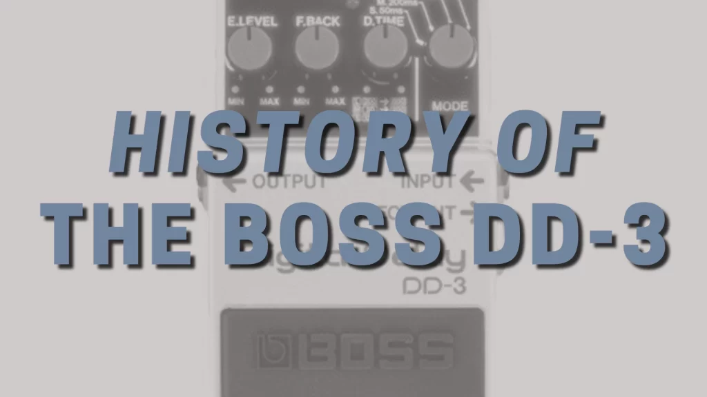
BOSS DD-3 Version History
DD-2 to DD-3 (1986)
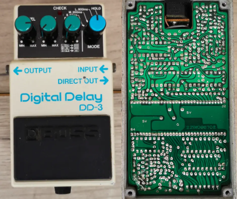
The BOSS DD-3 has it’s origins in a September 1986 service note for the BOSS DD-2.

According to Andreas Möller (aka Stinkfoot) the cost of manufacuring the DRAM chips became noticeably cheaper. So much so that BOSS decided to roll out the same DD-2 design at a lower cost, only under a new version name: the DD-3.
Introducing the DD-3A (1991)
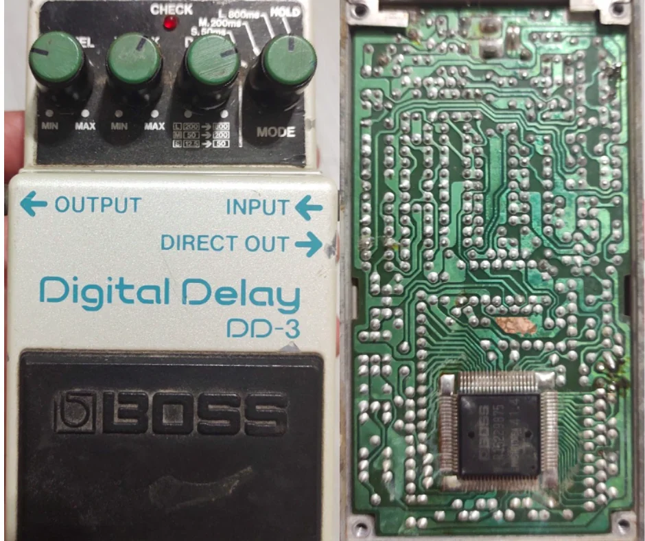
The service note for the second edition (called the BOSS DD-3A) dates back to April 1991. The document states that there is little difference in circuitry, but I found that to be untrue after reviewing the schematics.
DD-3 vs. DD-3A Circuit
The most obvious change is the decision to oust the long RDD63H101 custom chip in favor of a more compact gate array IC – the MN51010RBA. Nothing too novel here, except for some saved space and an upgrade to ASIC gate array technology.
The mode switch on the DD-3A ended up on the same circuit board as the other variable resistors. The original DD-3, on the other hand, had a separate board specifically for the Mode switch.
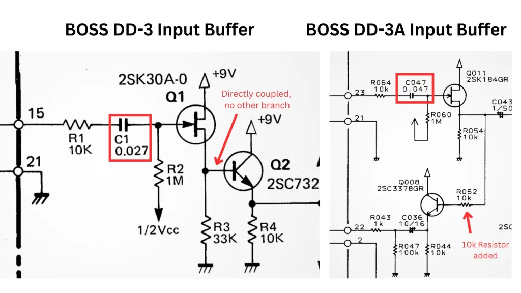
Going from left to right through the schematic, I was able to spot a small difference in the input buffer circuit. Specifically, the input signal in the DD-3A is routed directly from the JFET buffer. The DD-3 routed the input signal through a FET and a BJT buffer, in that order.
The DD-3’s C1 input capacitor was increased from 0.027uF to 0.047uF, while leaving the resistors equal – resulting in more low-end entering the DD-3A version.
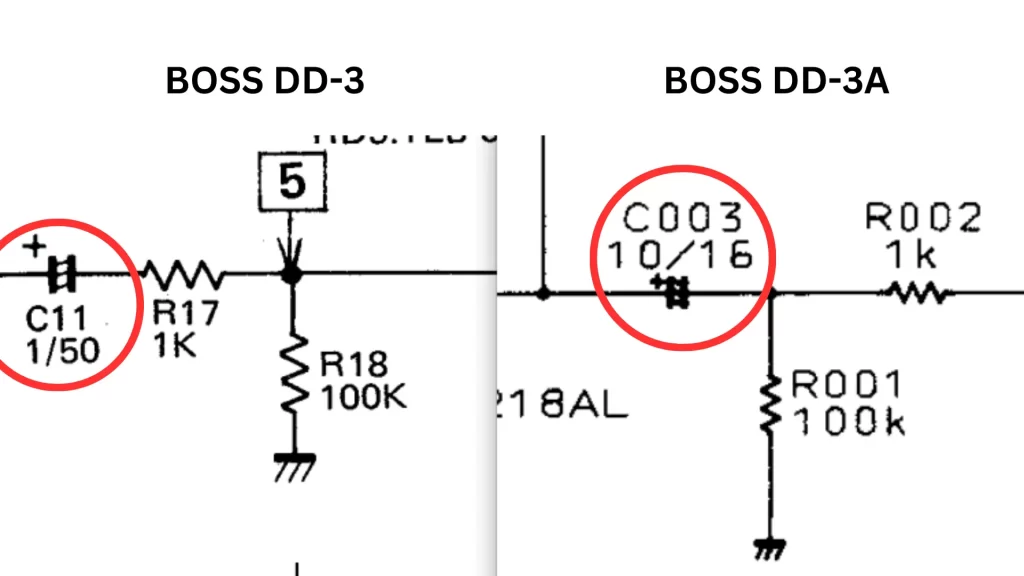
C18 was removed from the DD-3, allowing direct coupling between the Pre-Emphasis and the Compressor circuits in the DD-3A. This capacitor was most likely not needed.
Some of the electrolytics were changed from 10uF/50V to 1uF/16V.
Finally, BOSS decided to replace the three 64K DRAM chips with a single M5M4464L-12 DRAM chip.
How to Tell a BOSS DD-3 from a BOSS DD-3A
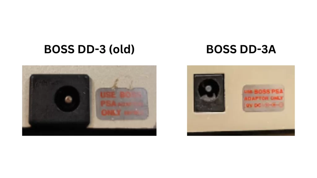
The DD-3A still uses the “DD-3” model code on the front face of the pedal. So, unless you know what to look for, it can be difficult to tell whether you’re looking at a DD-3 or a DD-3A. One way to tell a BOSS DD-3 from a 3A is the power connector. In the figure below the left power connector belongs to a first edition BOSS DD-3, while the right connector is from a BOSS DD-3A.
From the DD-3A to DD-3B (2002)
The service manual for the DD-3B version is dated May 2002. Confusingly, the service note is titled “BOSS DD-3(T)”, anything to make understanding this lineage more complicated to understand! The DD-3B is also the third version of the BOSS DD-3 series.
DD-3A vs. DD-3B Circuit
BOSS substituted the DD-3A’s M5M4464L-12 DRAM with a surface-mount M11B416256A-35T (the “(T)” in the service notes comes from the end of this part number). In the actual service notes, however, the part is referenced with “J(T)” at the end of the part number.
Looking at the DRAM datasheet reveals that “J” indicates a through-hole part and “T” indicates a surface-mount part. That leads me to believe that there may have been some DD-3B circuits built with the “T” version, and others built with the “J” version.
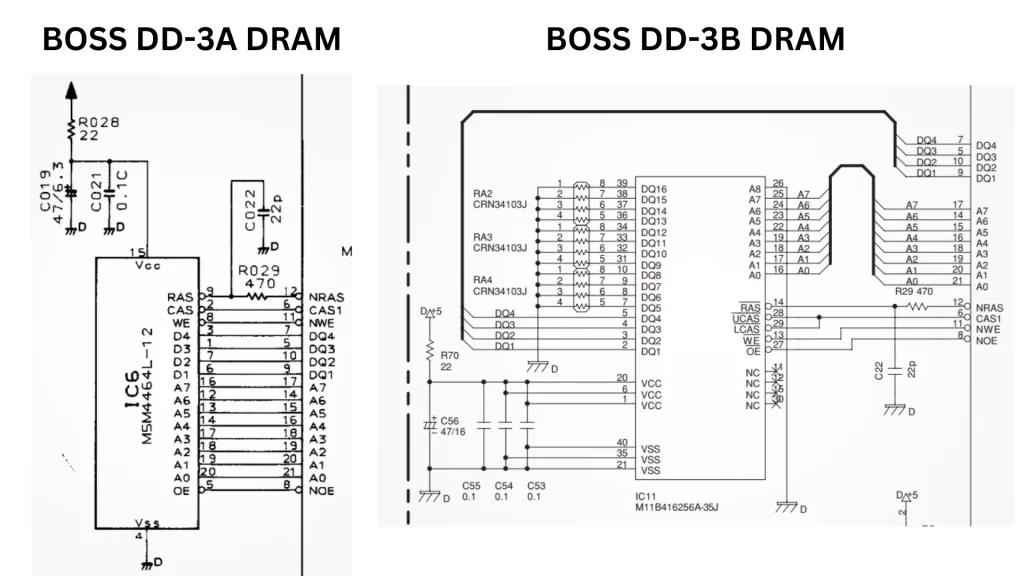
On top of this DRAM change, BOSS converted much of the circuit from through-hole parts to surface-mount. The gate array stayed the same between both versions.
How to Tell a BOSS DD-3A from a BOSS DD-3B
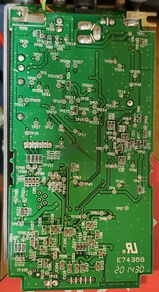
There are zero visual differences between the DD-3A and DD-3B! Luckily there are two other ways to tell: the serial number and the circuit board. According to the service notes, the DD-3B boards started appearing from 2001 onwards, with serial number SO91200 from the August 2001 1912LOT. Check the serial number using this online BOSS serial decoder.
The Current BOSS DD-3 Version (2014+)
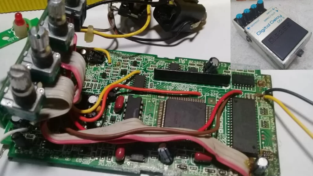
Around 2014 BOSS started manufacturing a fourth version of the DD-3. There is currently no schematic available, so we can’t comment on many detailed changes between the circuitry.
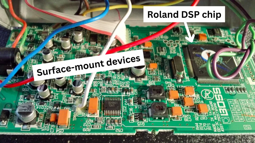
The biggest difference involves a move from DRAM-based digital delay to a new Roland DSP chip. Most of the components are surface-mount, and production is mainly carried out in Taiwan.
The BOSS DD-3T (2019)
In 2019, Roland announced that they were releasing a new version of the BOSS DD-3: the DD-3T. This version is equipped with a Tap Tempo input jack, which can be used with the BOSS FS-5U unlatched external footswitch for setting delay time.
Additionally, a mod exists for the DD-3T where a Tap Tempo switch is installed directly onto DD-3T, if desired.
Along with the DD-3T, Roland also announced the release of the new DD-8.
Meet the Author:

Hi, I’m Dominic. By day, I’m an engineer. By night, I repair and modify guitar effects! Since 2017, I’ve been independently modifying and repairing guitar effects and audio equipment under Mimmotronics Effects in Western New York. After coming out with a series of guitar effects development boards, I decided the next step is to support that community through content on what I’ve learned through the years. Writing about electronics gives me great joy, particularly because I love seeing what others do with the knowledge they gain about guitar effects and audio circuits. Feel free to reach out using the contact form!
The Tools I Use
As a member of Amazon Associates, Stompbox Electronics earns and is supported by qualifying purchases.


