In this post, we dissect what makes the BOSS VB-2 LFO circuit so unique. It doesn’t “fit in” with other oscillator circuits like relaxation oscillators, phase-shift oscillators, and Wein-Bridges. Read on for an in-depth look at modeling the VB-2’s LFO circuit, examining it’s behavior, and how we can modify it to suit our needs.

As a member of the Reverb Partner Program, eBay Partner Network, and as an Amazon Associate, StompboxElectronics earns from, and is supported by, qualifying purchases.
Disclaimer: Stompbox Electronics and/or the author of this article is/are not responsible for any mishaps that occur as a result of applying this content.
The BOSS VB-2 LFO
A low-frequency oscillator (LFO) is a circuit that generates a sub-audible signal. “Sub-audible” means that the oscillating frequency ranges from less than 1Hz up to 20Hz.
The most popular waveforms that the output signal can take include square, triangle, sawtooth, and sine. Large handfuls of circuits can be dug up and used to create an LFO, including relaxation oscillators, phase-shift oscillators, and Wein-Bridge oscillators.
The BOSS VB-2 LFO is distinct, though, as it doesn’t fall into any of the above oscillator circuits. Instead, it is based on a method of filtering a square wave into it’s fundamental sine wave frequency. Let’s take a look and see how this circuit works.
The VB-2 LFO Working Principle
The idea with the VB-2 LFO is to create a square wave, and then filter the fundamental frequency from that square wave. For example, if we had a square wave of 2Hz then it’s possible to filter it such that we end up with something like a sine wave of 2Hz.
But wait, filtering a square wave? Why does it make sense for us to filter a square wave?
Square Wave Frequency Composition
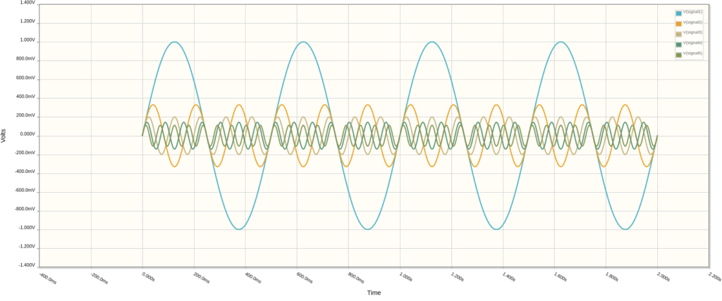
Square waves can be looked at as being built by adding up a bunch of sine waves. Let’s take a look at five different sine wave signals, based on the table below.
| Signal Name | Amplitude (V) | Frequency (Hz) |
|---|---|---|
| Signal 1 | 1 | 2 |
| Signal 2 | 1/3 | 6 (2Hz x 3) |
| Signal 3 | 1/5 | 10 (2Hz x 5) |
| Signal 4 | 1/7 | 14 (2Hz x 7) |
| Signal 5 | 1/9 | 18 (2Hz x 9) |
The amplitude decreases by 1/3 and 1/5 for signals 2 and 3, respectively. Similarly, the frequency increases by 3x and 5x for the same two signals. The same goes for the 4th and 5th signals. We can look at each one separately in the plot below.
Now, let’s add all the signals up to create one signal. The result is something resembling a wiggly square wave.
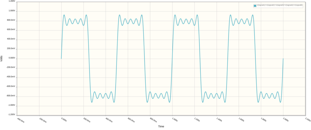
If we keep infinitely adding signals together with the same pattern then we’ll eventually end up with a clean square wave.
From Square Waves to “Sine” Waves
A sine wave can be recovered from a square wave by sending it through a band-pass filter. The filter needs to be tuned in order to extract it from the square wave. You can build a band-pass filter in many ways, but the simplest way (and frankly, the least efficient) includes using a low-pass RC filter and a high-pass RC filter in series.
A crude RC filter tuned for 2Hz would have R=1k and C=79.58uF.
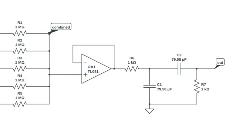
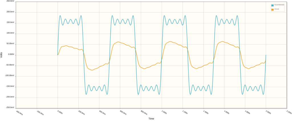
Remember, RC filters are not the most efficient! The output signal (orange) is far from a perfect sine wave, but accuracy isn’t the goal for this discussion. The idea is that a filter can be used to remove other frequencies from the square wave so that what’s left resembles a sine wave. The filter used in the VB-2 is more precise, as we’ll see.
An Overview of the VB-2 LFO Circuit
The LFO circuit has two main blocks: an Op Amp Filter and a Transistor Clipper.
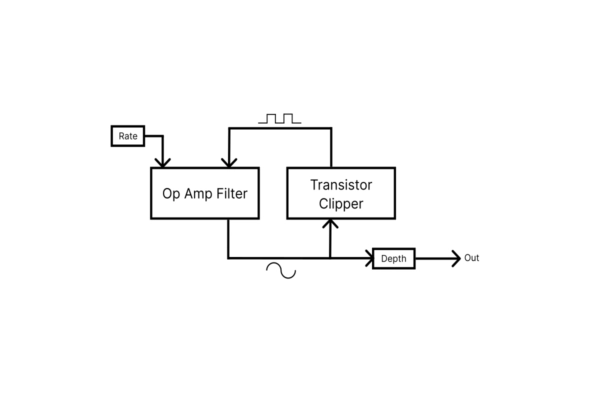
The Op Amp Filter takes the square wave generated by the Transistor Clipper and filters it into a sine wave. Then, the resulting sine wave is sent back to the transistor clipper which “clips off” the tops and bottoms of the sine wave to produce a square-like waveform. That square-like waveform is applied to the Op Amp Filter, and so on.
The Rate knob determines the frequency that the op amp filters out, which in turn determines the frequency of the LFO. The output of the Op Amp Filter gets fed into the Depth control, which attenuates the signal before being utilized by the rest of the vibrato circuit.
The VB-2 LFO Circuit
A schematic of the LFO circuit is shown below:
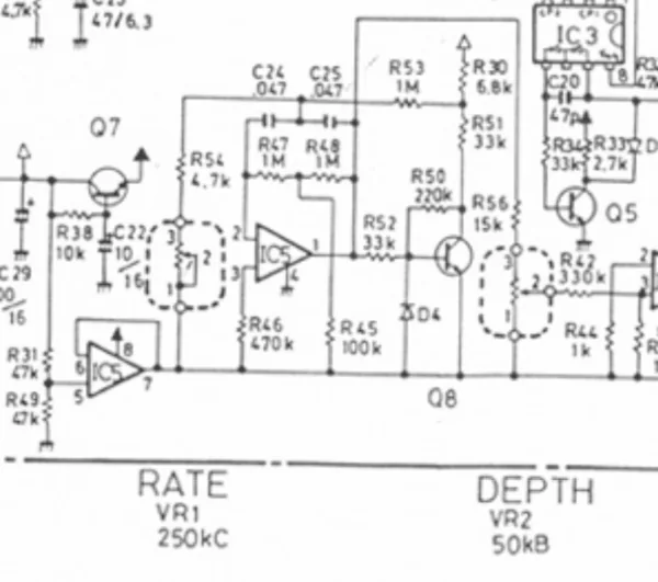
The LFO is composed of an op amp (IC5), a transistor (Q8), and a fistful of other passive components. After a short amount of time, the op amp produces a sine wave at its’ output, pin 1. That sine wave serves as the output of the LFO which travels through R56 into potentiometer VR2 (used as an attenuator for depth control).
Additionally, that same sine wave at pin 1 travels through R52 to the base of Q8. The diode D4 and the base-emitter junction of Q8 both serve to form a square wave at the transistor base by hard clipping the sine wave. The resulting square-like waveform becomes amplified by the common-emitter configuration of Q8 and can be monitored at the collector terminal.
The amplified square wave feeds back into the op amp’s inverting input, pin 2, through resistor R53. The op amp’s feedback network is set up as a bridged-T network (formed by R47, R48, R45, C24, C25, R54, and VR1). This bridged-T network, in conjunction with the op amp, forms a tuned filter with VR1. In effect, VR1 controls the frequency at which the filter operates.
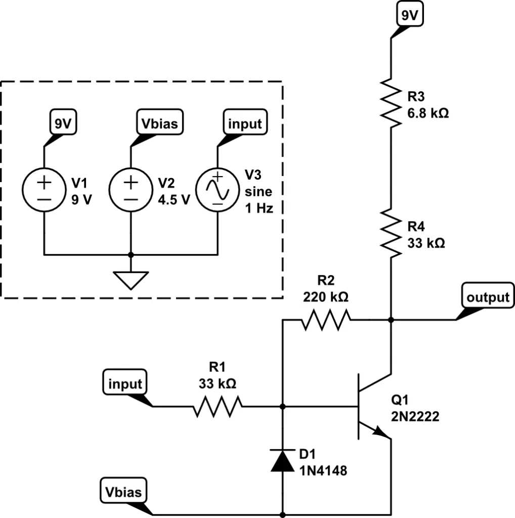
Transistor Clipper Circuit
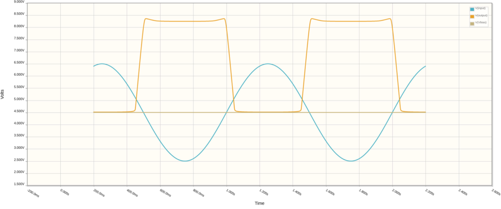
I’ve modeled the Transistor Clipper circuit in the schematic below. An input signal of 1Hz is applied. The bias voltage (Vbias) is set to half the supply (9V/2 = 4.5V). After the signal travels through R1 it reaches D1 and the base of Q1. Both of these devices apply hard clipping to the sine wave. The clipped signal shows up at the collector, as can be seen in the plot below.
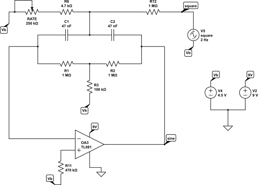
Op Amp Filter
I’ve modeled the Op Amp Filter below. The square wave is simulated as V5 with a frequency of 2Hz. Like before, the bias voltage (Vb) is half the supply voltage.
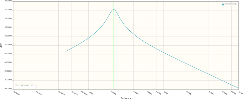
A frequency analysis of the op amp filter reveals that the circuit acts as a band-pass filter with a strong Q factor.
The plots in the following sections were made by sweeping the frequency of the square wave (V5) and recording the magnitude of the output signal (‘sine‘). As the frequency increases, the amplitude of the sine wave increases until it peaks at a specific center frequency. Then, it rapidly falls off. In fact, the center frequency of the band-pass filter determines the oscillation frequency of the LFO.
Additionally, the frequency at which the filter operates can be adjusted by a simple resistance value (the RATE pot). Capacitors C1 and C2 also affect the oscillation frequency.
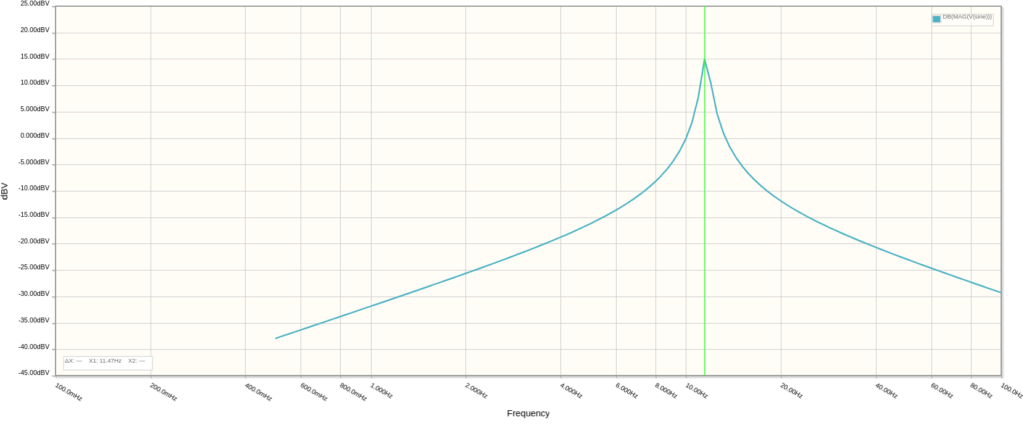
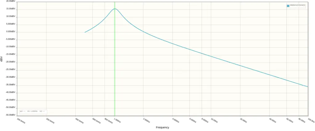
Frequency-Magnitude Plots (Adjusting the Rate knob)
Firstly, with the RATE + R6 resistance at maximum, the op amp filter has a center frequency of 2.178Hz:
And taking the RATE resistance to zero, the center frequency increases to around 11.47Hz:
Frequency-Magnitude Plots (Adjusting C1 and C2)
Let’s return the RATE knob to its’ full resistance and start adjusting the capacitors C1 and C2. First, let’s increase C1 to 100nF. The peak frequency decreases to 1.489Hz.
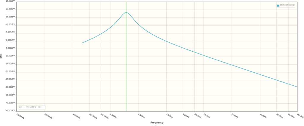
Returning C1 to 47nF and changing C2 to 100nF produces the same frequency response. That’s not too suprising, given the symmetry of the bridged-T network. Next, we’ll increase both caps to 100nF and keep the RATE knob unchanged.
Modeling the Entire LFO Circuit
I’ve modeled the enture LFO circuit below:
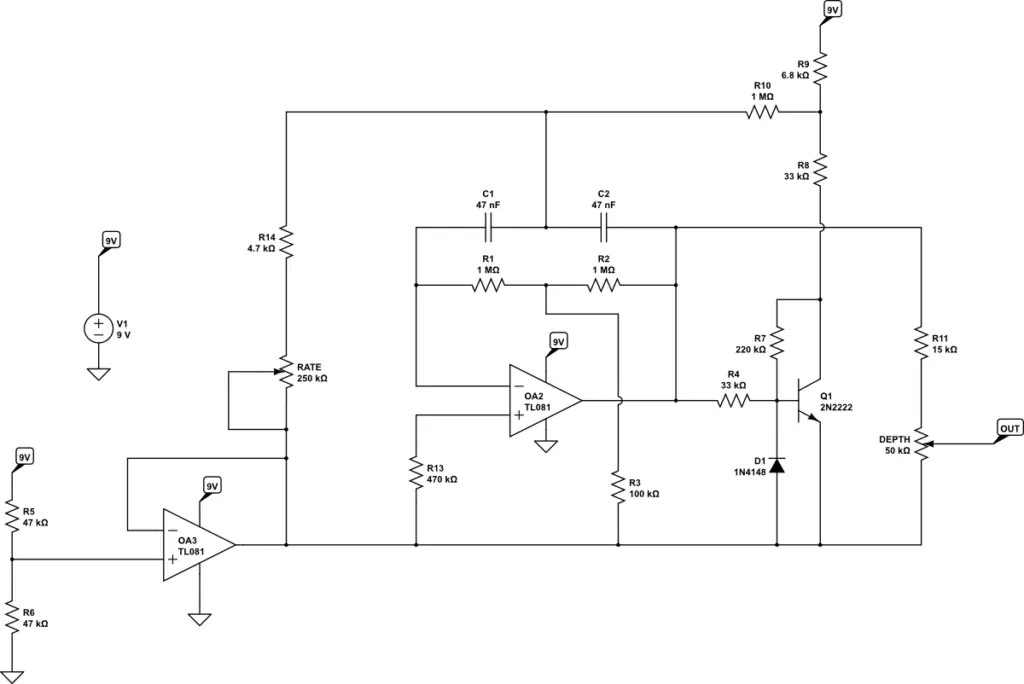
Circuit Waveforms
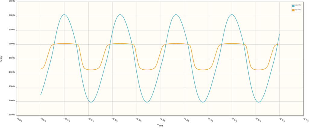
The output of the op amp output (blue) passes through R4 and becomes clipped at the base of transistor Q1 (orange).
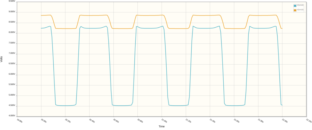
Q1 amplifies the clipped signal at the collector (blue), which then becomes attenuated by the divider formed by R8 and R9 (orange).
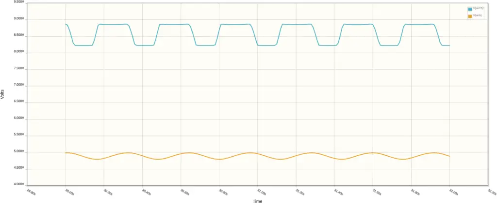
Next, by way of R10, the attenuated square wave signal (blue) affects the voltage at the node between capacitors C1 and C2 (orange). If the resistance from the RATE + R6 is large, then the time it takes for the voltage at the C1/C2 node to change increases. This is because, with the added resistance, it takes longer for the capacitors to charge and discharge.
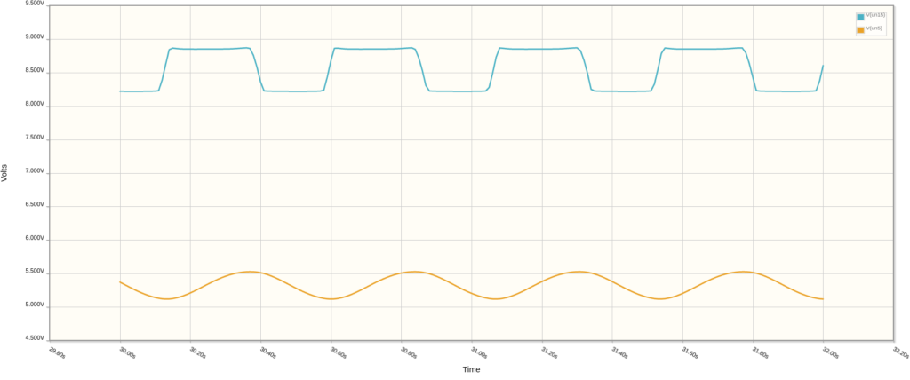
Additionally, lowering the resistance of the RATE + R6 branch makes it easier for C1/C2 to charge and discharge, increasing the frequency of oscillation.
Meet the Author:

Hi, I’m Dominic. By day, I’m an engineer. By night, I repair and modify guitar effects! Since 2017, I’ve been independently modifying and repairing guitar effects and audio equipment under Mimmotronics Effects in Western New York. After coming out with a series of guitar effects development boards, I decided the next step is to support that community through content on what I’ve learned through the years. Writing about electronics gives me great joy, particularly because I love seeing what others do with the knowledge they gain about guitar effects and audio circuits. Feel free to reach out using the contact form!
The Tools I Use
As a member of Amazon Associates, Stompbox Electronics earns and is supported by qualifying purchases.