
The PROTIS 1 Guitar Effects Development Board can be used for prototyping and testing out various DIY guitar effects circuits. This post provides an example circuit, the common Transistor Buffer, to highlight basic functionality offered by the PROTIS 1. In this post you will learn how to utilize the Power section and the Input/Output (I/O) connections.
Get ready for an introductory dive into what the PROTIS 1 can offer!
Disclaimer: Stompbox Electronics and/or the author of this article is/are not responsible for any mishaps that occur as a result of applying this content.
Parts List
| Part | Qty | Where to Buy |
|---|---|---|
| 2N3904 Transistor (or equivalent) | 1 | Mouser | Amazon | Tayda |
| 0.1uF Capacitor | 2 | Amazon | Tayda |
| 1 MOhm Resistor | 3 | Amazon | Tayda |
| 10k-Ohm Resistor | 1 | Amazon | Tayda |
You will also need:
- PROTIS 1 Guitar Effects Development Board
- Male-to-Male Jumper Wires (provided optionally with the PROTIS 1)
- 18VDC Center-Negative Power Supply (provided optionally with the PROTIS 1)
- One (1) 0.2″ Shunt (provided with the PROTIS 1)
- One (1) 0.1″ Shunt (provided with the PROTIS 1)


Transistor Buffer Schematic
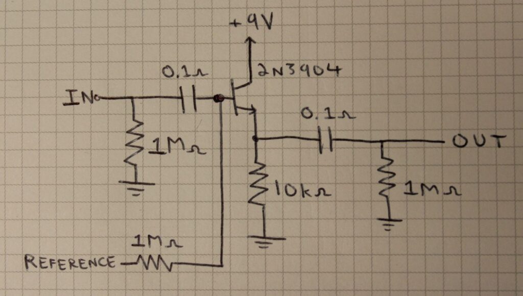
Power Configuration
Power is supplied by an 18VDC Power Supply (provided) and plugs into the power jack (J1) at the upper-right corner of the board. This supplies power to the right-hand side of the POWER DISTRIBUTION header, as well as the “+18VDC” access points at both of the POWER BUS headers.
Please do NOT plug in the +18VDC power supply until we have built the circuit on the breadboard and have double-checked our connections!
From the schematic, it looks like we will need +9V in order to power our circuit. To make the +9V available for use, we’ll have to first activate the “+9V” access point at the POWER BUS headers.
To do so, grab a 0.2″ shunt (provided) and jumper the +9V option at the POWER DISTRIBUTION header. This supplies +18V to the 7809 regulator, which then supplies +9V to the “+9V” access point at the POWER BUS header.
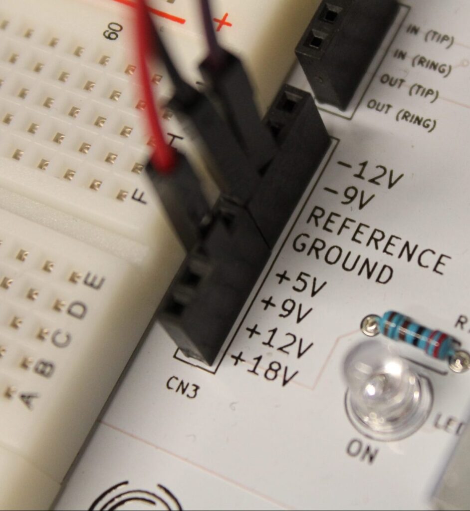
The ground for our circuit is accessible from the the POWER BUS header’s “GROUND” pins. Locate the “+9V” and “GROUND” pins and route them to separate bus lines on the breadboarding space using the Male-to-Male jumper wires (provided).
Reference Voltage
Now that we have our power signals set up, we will need to generate our bias voltage (labelled “REFERENCE” in our schematic).
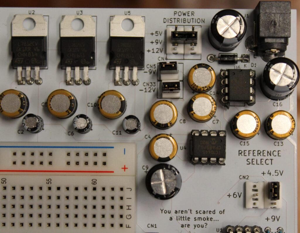
The bias voltage reference is generated by configuring the REFERENCE SELECT header (see Figure 1). Looking at the header, there are three options: +4.5V, +6V, and +9V. Always choose the option that is half of your circuit’s power voltage.
In our case, we should choose +4.5V since this is half of +9V. Grab a 0.1″ shunt (provided) and jumper the middle pin and the +4.5V pin of the REFERENCE SELECT header. This activates the “REFERENCE” pin on the POWER BUS headers. Locate the “REFERENCE” access point and route this signal to a different bus line on the breadboarding space.
Always double-check your power connections when using the PROTIS 1!
Building the Transistor Buffer
Now that all the power is set up you can start building the circuit! Use the schematic above for reference. Don’t worry about the IN and OUT signals yet, we will hook those up in the next section.
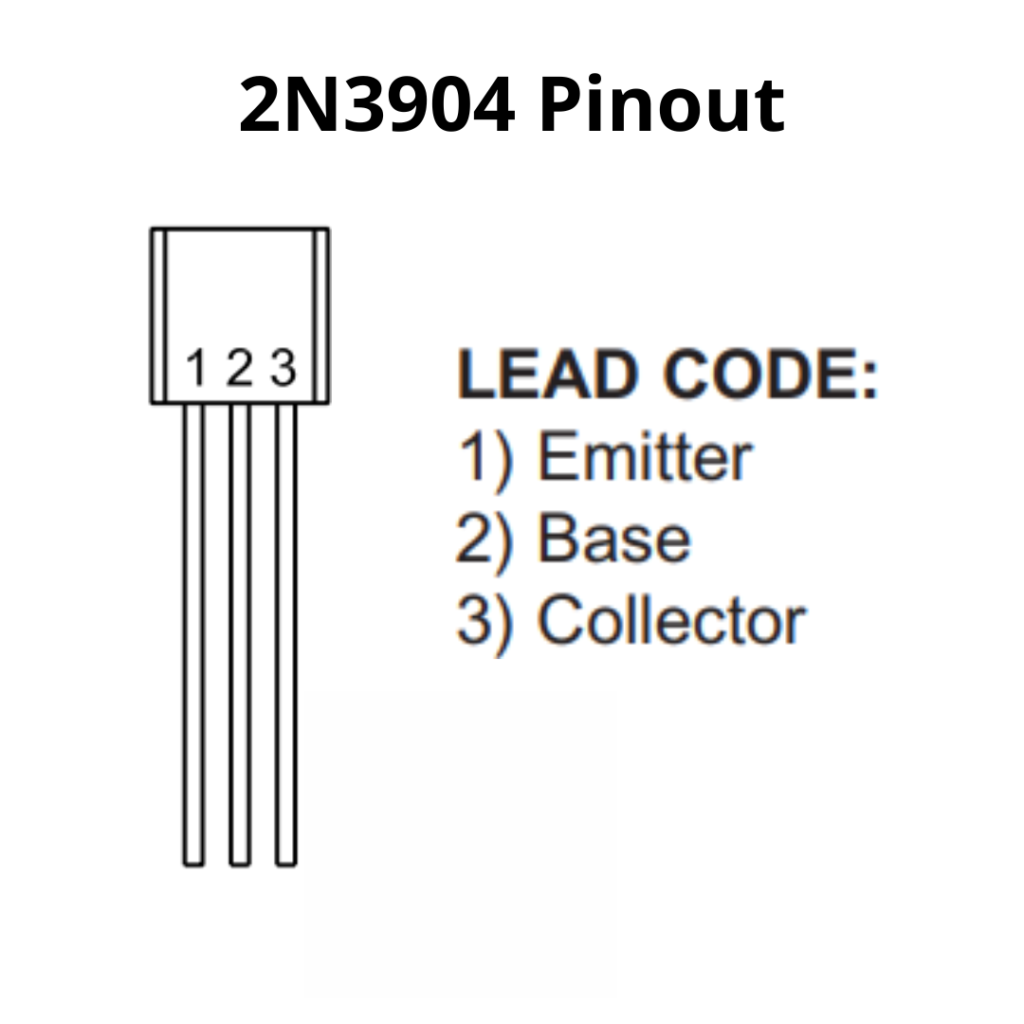
Also, be aware of the transistor pinout (Which pin is the base? The Emitter? Collector? How are they depicted in the schematic?). To answer these you will need to look up the datasheet for the transistor you are using (in this case, the 2N3904). Looking up datasheets is a good skill to have when working on electronics, do not underestimate this!
Once we have hooked up all the components according to the schematic we can move onto the next step: connecting the input and output jacks.
Connecting the Guitar and Amplifier
The Input Jack (J3) is the 1/4″ jack on the right side of the board. The Output Jack (J2) is on the left side. Connect your guitar input to the Input Jack and the Amplifier to the Output Jack.
To access the Input (Guitar) and Output (Amplifier) connections, utilize the “IN (TIP)” and “OUT (TIP)” pins on the I/O BUS headers. These are located on both sides of the breadboarding space for easy access.
The IN signal on the schematic routes to the “IN (TIP)” pin and the OUT signal, to the “OUT (TIP)” pin. Use Male-to-Male jumper wires to connect these signals as per the schematic.
Double-Checking the Circuit
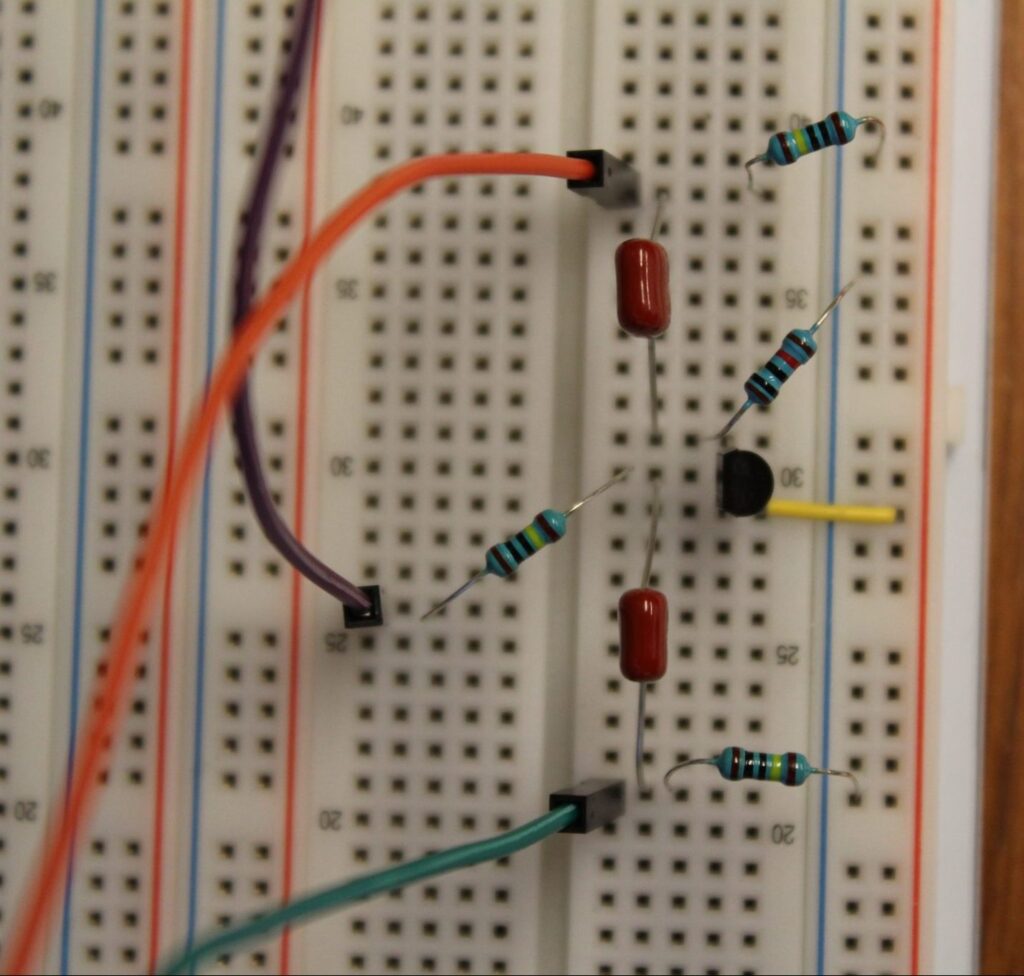
As emphasized, always double-check that the wiring and components are set up exactly as the schematic shows. Consult Figure 3 below to see an overhead view of the breadboarded transistor buffer.
Here are a couple of questions to ask yourself before providing power to the board:
- Does each power rail and reference voltage have their own, separate bus line on the breadboard?
- Is the power distribution configured properly in the POWER section?
- What is the pinout of the transistor we’re using? Is it connected just like how the schematic shows?
- Are any of the long-leaded component (resistors, capacitors, etc.) leaning on an adjacent component? If their leads are touching, then move the leads slightly so they don’t cause any unwanted shorts.
- Are the IN and OUT signals going to the input and output of the circuit, respectively?
Testing the Buffer
We’ve double-checked our work and are ready to turn this thing on!
Plug the +18VDC power supply into the power jack (J1). Now, turn on your amp and play. By default, the PROTIS 1 comes in BYPASS mode, so you should be hearing your guitar’s DRY signal. To ENGAGE the PROTIS 1, simply press the “TRUE BYPASS SWITCH.” Now when you play, you should hear the output of the Transistor Buffer circuit you just built…from the ground up!
Meet the Author:
Hi, I’m Dominic. By day, I’m an engineer. By night, I repair and modify guitar effects! Since 2017, I’ve been independently modifying and repairing guitar effects and audio equipment under Mimmotronics Effects in Western New York. After coming out with a series of guitar effects development boards, I decided the next step is to support that community through content on what I’ve learned through the years. Writing about electronics gives me great joy, particularly because I love seeing what others do with the knowledge they gain about guitar effects and audio circuits. Feel free to reach out using the contact form!