
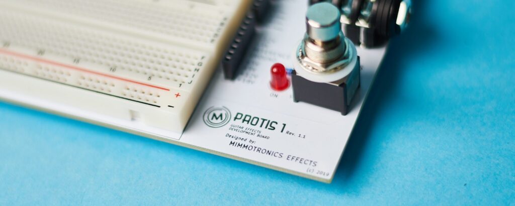
One of the most important parts of building your DIY guitar pedal is figuring out how to apply power to your circuit. The required voltages are generally standardized across the industry as +18V, +12V, and (most commonly) +9V. All three of these voltage levels are supported by the PROTIS 1 development board.
Other voltages are also available, like +5V and other negative voltages, but the reasoning for including those in the design may be a mystery to you. This article should clear that up and better explain how to use each of the power options available on the PROTIS 1 board.
Disclaimer: Stompbox Electronics and/or the author of this article is/are not responsible for any mishaps that occur as a result of applying this content.
Analog vs. Digital Components
There are two types of components that require power in any given DIY guitar effects circuit:
Analog components consist mainly of operational amplifiers (op amps) and transistors. For simplicity, we will only consider analog circuits with operational amplifiers for this post, since the reasoning is the similar for transistor circuits.
Digital components include digital digital integrated circuits (ICs), microcontrollers (uC), DSP chips, and any other components exclusively involved in digital design.
Powering Analog Circuits
Analog circuits commonly consist of transistors and operational amplifiers. These are active components, so by definition they require power.
There are two main design methods for supplying power to operational amplifiers:
- Dual-supply
- Single-supply
By far the most popular in guitar pedal design is the single-supply approach. That said, each of them have their own benefits and pitfalls, and we’ll skim over some of them in this article.
Dual-Supply Design
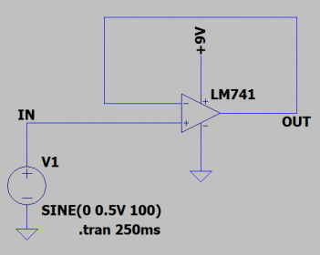
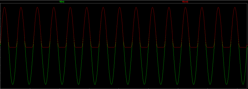
The best way to explain these concepts is by example. Consider the circuit in Figure 1, which shows an op amp buffer circuit powered by two voltage levels: +9VDC and -9VDC. It was created with a program called LTSpice, which is used to model circuits before building them.
The input signal (V1) is a sine wave, modeled as SINE(0 0.5V 100). In this model, the signal varies with respect to 0V between -0.5V and +0.5V.
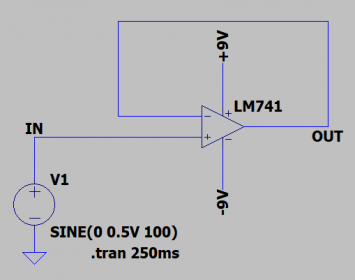
In total, the signal is allowed to swing between the power levels -9V to +9V, which is quite substantial considering the guitar signal varies much lower than that. This high “headroom” characteristic has implications when designing overdrives and boost circuits.
Dual-Supply Power Options on the PROTIS 1
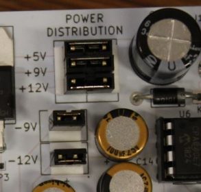
The PROTIS 1 offers both +9VDC and -9VDC, as well as +12VDC and -12VDC. This gives you two options if you ever run into the need for a dual-supply power approach. The power rails are located on the right-hand side of the breadboarding space (the POWER headers).
The negative power rails are enabled by placing a jumper across the male headers labelled with the inverted voltage you are seeking. See Figure 2 as a reference.
Absolute Maximum Ratings
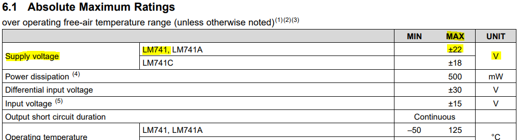
Some important specifications for a given op amp are given as Absolute Maximum Ratings in the datasheet. When you use op amps, make sure that the voltage difference across the power supply rails doesn’t exceed the absolute maximum rating.
For example, the circuit in Figure 1 is powered from +9V and -9V. The total voltage difference between the two rails is +9V – (-9V) = 18V. The LM741 op amp has an absolute maximum supply voltage rating of 22V, according to the datasheet. Therefore, the design above is in the acceptable operating range.
Single-Supply Design
Single-Supply design is quite different from dual-supply design. What defines single-supply design is the use of one (1) non-zero voltage rail. The other rail is considered to be the circuit’s ground at 0VDC.
Consider the design in Figure 4a. Again, we have an op amp buffer circuit that operates in the same way as the circuit in FIGURE 1. In this case, only one supply rail powers the op amp.
However, this circuit is WRONG. Look at the waveform in Figure 4b, the signal in GREEN is the input signal being applied to the op amp. The RED signal is the resulting output from the op amp.
Both of these signals should be clean sine waves, but since the input signal is biased to a 0VDC reference, and because the lower voltage rail of the op amp is 0VDC, the negative portion of the signal cannot pass through the circuit. This results in only the positive side of the input signal being reproduced at the output.
Biasing in Single-Supply Designs
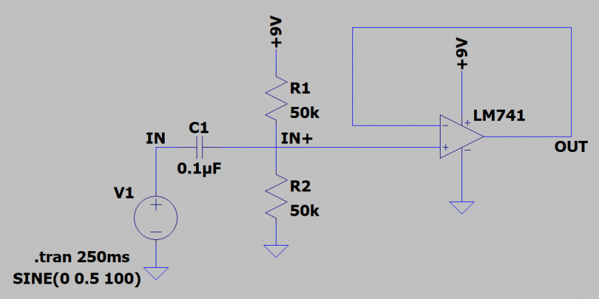
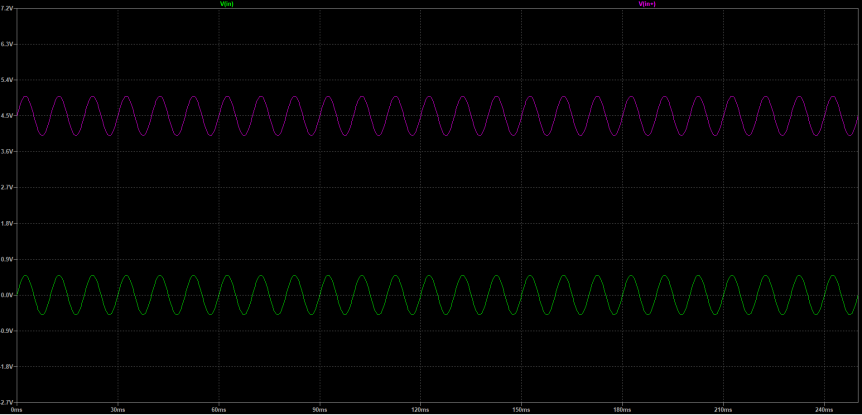
To fix this issue and to re-obtain the negative portion of the signal, we need to bias the input signal such that the entire signal range can be reproduced within the power supply rails (between 0VDC and 9VDC). The bias voltage that offers the best possible solution is 4.5VDC. At this operating point we will have 4.5V of headroom in both the positive and negative directions.
To do this we can introduce two resistors (R1 and R2 in Figure 5a), forming a voltage divider. This introduces a correctly biased signal at the input terminal of the op amp. We also need to introduce a blocking capacitor (C1) to protect our bias voltage from changing.
At this point I think you realize one downside to using Single-Supply designs: you need to introduce more components to bias the signal within the positive voltage range. In dual-supply designs we didn’t have to do that. So, what are we talking about this for if it’s so much more complicated?
Well, using one power supply rail is usually much simpler when it comes to power supply design. With dual-supply, you have to worry about creating the negative voltage rail. Not only that, you have one more power rail to route across your circuit board. That’s not always an easy thing to deal with when dealing with audio.
On the flip-side, dual-supply designs have the potential to offer much more headroom than single-supply designs. Whichever design you choose is completely based on the application.
Powering Digital Circuits
The PROTIS 1 allows for the prototyping of digital circuit designs by providing +5VDC (shown in Figure 2). This will power most of the 4000 series integrated circuits, as well as most microcontroller chips, like PIC or Atmel.
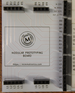
Remember that many digital circuits today run on 3.3VDC, so check the datasheets for absolute maximum power supply ratings before applying +5VDC to your circuit. The PROTIS 1 does not inherently accommodate for digital circuits running on +3.3VDC, since this is not so common in the DIY community. However, if you need +3.3VDC as a power source, then you may build a converter circuit using the Modular Prototyping Board space to the left-hand side of the board (Figure 6).
Meet the Author:

Hi, I’m Dominic. By day, I’m an engineer. By night, I repair and modify guitar effects! Since 2017, I’ve been independently modifying and repairing guitar effects and audio equipment under Mimmotronics Effects in Western New York. After coming out with a series of guitar effects development boards, I decided the next step is to support that community through content on what I’ve learned through the years. Writing about electronics gives me great joy, particularly because I love seeing what others do with the knowledge they gain about guitar effects and audio circuits. Feel free to reach out using the contact form!