Whether you’re a DIY enthusiast looking to build your own LPB-1 clone or just curious about it’s inner workings, this article highlights valuable insights that you can take away and put into practice.
We’ll take you on a deep dive into the design of this classic booster circuit, exploring its components, topology, and technical characteristics. You might get a few modification ideas along the way!

As a member of the Reverb Partner Program, eBay Partner Network, and as an Amazon Associate, StompboxElectronics earns from, and is supported by, qualifying purchases.
Disclaimer: Stompbox Electronics and/or the author of this article is/are not responsible for any mishaps that occur as a result of applying this content.
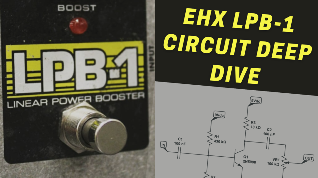
LPB-1 Circuit Overview
First, let’s look at the basic LPB-1 circuit that floats around the interwebs, shown below.
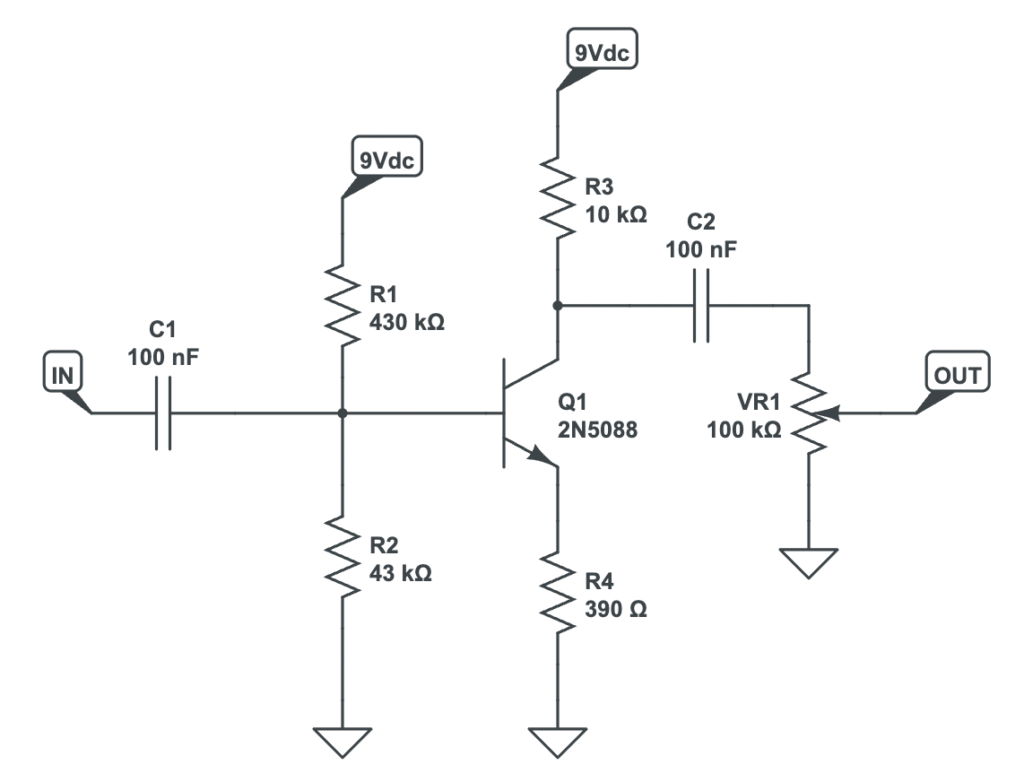
The LPB-1 guts are centered around a 2N5088 NPN transistor, surrounded by a handful of resistors for biasing. Two coupling capacitors are used to let in and out the guitar signal. They also serve to block any DC voltages from entering or leaving the amplifier circuit.
The pedal is powered by 9Vdc via an adapter or battery. When using a battery you need to insert a plug into the pedal’s input jack in order to make the ground connection. Series diode protection is accomplished with a 1N4001 rectification diode. If that diode dies for some reason, you can find a replacement on Amazon or from any electronics parts distributor like Mouser, DigiKey, etc.
The actual LPB-1 design includes three passive RF low-pass filters, each composed of one (1) 100pF ceramic capacitor and one (1) inductive ferrite bead. One of the filters is placed near the power jack and the other two are used near the input and output jacks.
Mod Opportunity
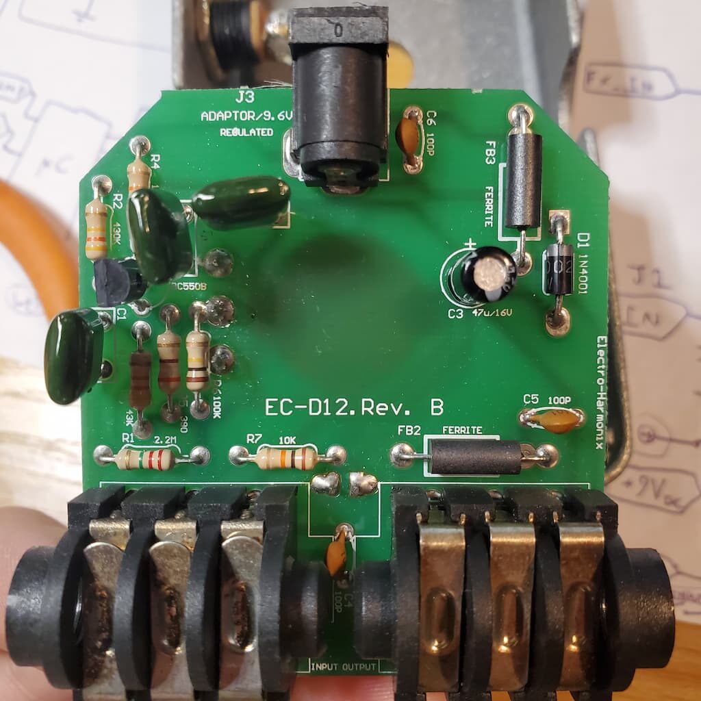
A common mod is to remove the 100pF capacitors (only C4 and C5) with electrical snips. Some have reported that the tone clears up after performing this mod. However, those capacitors are there to keep out radio frequencies, so don’t be surprised if you start hearing local stations playing through your amp!

The 2N5088 Transistor
At the heart of the LPB-1 schematic you’ll find the 2N5088 NPN bipolar junction transistor (BJT).
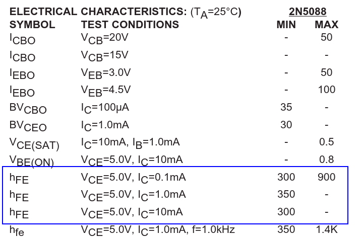
Transistors have a parameter called beta (hFE), which reflects the amount of current gain produced by the transistor. Beta is also described as the collector current divided by the base current of the transistor.
Beta, like most gain values, is unitless and can be found in the datasheet of the transistor. Every transistor has a unique beta, even among like-models. Generally, though, the range of possible beta values for a given transistor type allows you to differentiate between them.
For a 2N5088, the beta can be very high: between 300-900. For the BC550B (the one in my LPB-1 pedal) the beta ranges between 200-450, according to its datasheet. Conversely, the range of beta for a 2N3904 is about 100-300. The 2N4401 transistor beta range extends a tad lower than the 2N3904: around 80 at the minimum up to 300.
Mod Opportunity
The LPB-1 uses transistors that are similar to the 2N5088. For example, the LPB-1 in the photo above uses a BC508B. Knowing that you can use different, but similar, transistors, one modification idea is to try out different transistor models. Experiment with other BJT NPNs that have a similar pinout (1 = Collector, 2 = Base, 3 = Emitter) to see if they have an affect on the tone.

LPB-1 Circuit Configuration
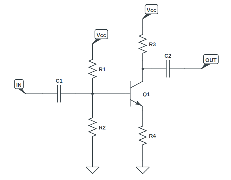
The LPB-1 uses a common configuration in electronics called the Common-Emitter (CE) Amplifier. In this configuration, a transistor is used to boost a signal being applied to it’s base terminal. That signal modulates the current flowing into the collector and is converted into a voltage via R3 that can be accessed at the collector terminal.
Below is the same LPB-1 circuit without the component values to illustrate the “shape” of the Common Emitter configuration:
Resistors R1 & R2
Resistors R1 and R2 are used to bias the DC voltage at the base terminal. The biasing is needed so the signal has enough room to “wiggle” around a voltage level that is within the bounds of 0Vdc and the supply voltage.
Resistors R3 & R4
R3 and R4 determine the voltage gain of the circuit. It’s important to note that a change in R3 will have an effect on the DC bias of the collector terminal. If you modify R3, then you will need to make sure that the bias point at the collector terminal is still far enough away from the supply rails to avoid clipping.
Capacitors C1 & C2
The capacitor C1 couples an input signal to the input of the amplifier and serves to remove any DC bias on the input signal. As a result, all the DC biasing for the LPB-1 can be done without being influenced by outside factors. Likewise, capacitor C2 is used to remove the DC voltage from the output of the amplifier so that only the signal is passed to the output jack.
Common-Emitter Calculator Tool
The Stompbox Electronics Common-Emitter Amplifier calculator (below) allows you to see what happens when modifying certain values in the CE circuit. The calculator defaults to the values used in the LPB-1 circuit, so you can simply click “Calculate” to generate the voltage and current values. Then, play around with different resistances and transistor betas to see how they would affect the measurements.
Common-Emitter Equations
The equations used for calculating the voltages and currents in a Common-Emitter amplifier circuit are relatively complicated, but there are some “rule of thumb” equations that can be useful.
For a more in-depth overview, head over to our Common-Emitter calculator page and scroll down to see the mathy breakdown.
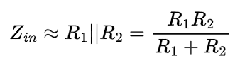
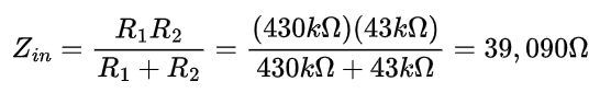
Common-Emitter Input Impedance
The input impedance of a common emitter circuit is the parallel combination of R1, R2, and the impedance looking into the base. For a CE amp, the impedance looking into the base terminal is the emitter resistance multiplied by the transistor beta.
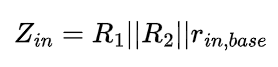
Usually, the multiplication of the transistor beta and emitter resistance is so large that it can be ignored in the input impedance calculation. As a general rule of thumb, use the simplified calculation of R1 || R2.
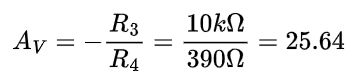
Common-Emitter Gain
For common-emitter amplifiers, computing the gain is fairly straightforward. Just divide the collector resistance by the emitter resistance. Then, multiply by -1:
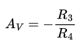
The negative sign indicates that the output signal is an amplified “negative version” of the input signal. That just means if the input signal goes up, the amplified output signal will go down (and vice-versa).
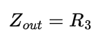
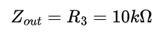
Common-Emitter Output Impedance
The output impedance of a common-emitter amplifier is the parallel combination of the collector resistor and the impedance looking into the collector terminal. The impedance into the collector terminal is very high, so we can simply use the collector resistor as the value for the output impedance.
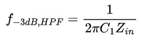
Input High-Pass Filter Cut-Off Frequency
The input coupling capacitor, C1, forms a passive high-pass filter with the input impedance of the amplifier. Usually the value for C1 is chosen to allow the lowest frequency-of-interest into the circuit without impeding it. That minimum frequency can be calculated using the cut-off frequency equation for a high-pass filter circuit:
LPB-1 Circuit Analysis
Now that we have some common-emitter equations jotted down we can start applying them to the LPB-1 circuit! Not only will these serve as a benchmark for other designs; they can also give us insight on where to make some interesting modifications!
Input Impedance
LPB-1 Circuit Gain
The gain of the common emitter amplifier is simply the collector resistance divided by the emitter resistance:
Output Impedance
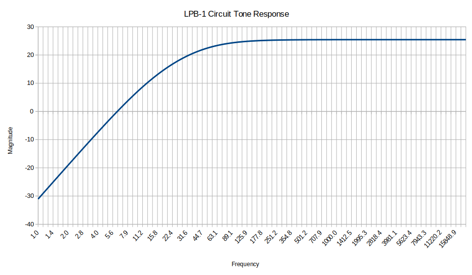
LPB-1 Frequency Response
The cut-off frequency for the high pass filter formed by C1 and the input impedance works out to approximately 40 Hz.
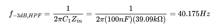
But remember, we left out the base-terminal impedance when calculating the input impedance value. So, the real impedance is actually lower than 39k. As a result, the real cut-off freqency is slightly higher than 40Hz. In fact, it’s more like 54 Hz.
I used CircuitLab to simulate the tone response of the LPB-1’s output below. The cut-off is centered at around 54 Hz.
Mod Opportunity
The lowest frequency on a bass guitar sits around 41 Hz. If you’d like to modify the LPB-1 for bass guitar, one suggestion would be to increase the C1 and C2 capacitors to between 150nF – 220nF. After doing so you’ll end up with a cut-off frequency of between 36Hz – 24Hz, respectively, on the input. After doing so you’ll have a proper clean boost for all bass guitar frequencies.

Meet the Author:

Hi, I’m Dominic. By day, I’m an engineer. By night, I repair and modify guitar effects! Since 2017, I’ve been independently modifying and repairing guitar effects and audio equipment under Mimmotronics Effects in Western New York. After coming out with a series of guitar effects development boards, I decided the next step is to support that community through content on what I’ve learned through the years. Writing about electronics gives me great joy, particularly because I love seeing what others do with the knowledge they gain about guitar effects and audio circuits. Feel free to reach out using the contact form!
The Tools I Use
As a member of Amazon Associates, Stompbox Electronics earns and is supported by qualifying purchases.