By: Dominic Sciarrino | Stompbox Electronics | Last Updated: February 25th, 2026
As a member of the Reverb Partner Program and as an Amazon Associate, StompboxElectronics earns from, and is supported by, qualifying purchases.
Disclaimer: Stompbox Electronics and/or the author of this article is/are not responsible for any mishaps that occur as a result of applying this content.
Introduction
If you’ve ever built a true bypass pedal, you’ve probably heard a loud thump or pop the moment you engage the switch. It’s one of the most common problems in DIY pedal design, and it has a specific, well-understood cause … and a well-understood fix.
The De-Popper isn’t a traditional effect circuit. It’s a set of components added to a true bypass circuit to suppress the switching sound. But understanding why those four components work means understanding two fundamental components that appear in virtually every pedal circuit you’ll ever build: the capacitor and the resistor.
This article introduces both. If you’ve never worked with capacitors before, this is the best possible context – a real problem with a clear solution, explained from the ground up.
Part 1: What Causes Switch Pop?
There are two separate sources of switching noise in a true bypass pedal. Most builders only know about the first one. Both need to be addressed for reliable, quiet switching.
Source 1: DC Offset
What is an AC Signal?
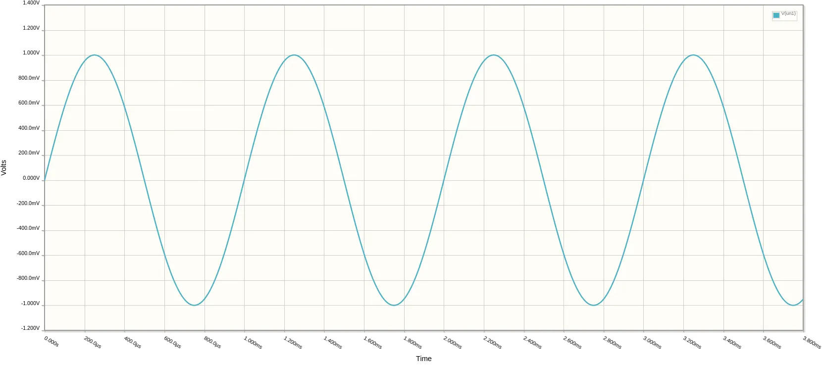
Your guitar signal is an AC signal. It’s a time-varying voltage that moves continuously above and below a center reference point, which in a pedal is usually ground (0V). A sine wave is the textbook example. Your guitar doesn’t produce a perfect sine wave, but it’s the same principle: a voltage that oscillates around zero.
The key property is that your guitar signal carries no DC component. On average, it sits at zero volts. It doesn’t carry a fixed offset above or below ground.
Where the Pop Comes From
Even when it’s doing nothing, your effect circuit may have a small DC voltage present at its input or output nodes. Capacitors inside the circuit can accumulate charge over time. Junction leakage across transistors and op-amps can establish a small static potential. That potential sits quietly on the circuit’s input or output node while the pedal is in bypass mode.
When you engage the pedal, the switch suddenly connects that DC-offset node to your signal path. The voltage difference between the node and the signal path equalizes extremely quickly. That rapid voltage change propagates through your signal chain, and you amplifier amplifies it.
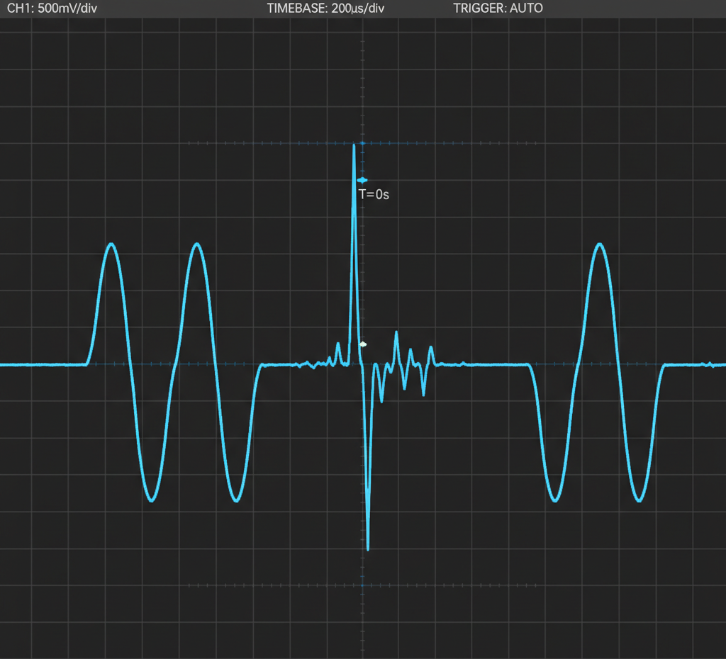
Research from pedal builders has found that any DC offset above approximately 5mV (0.005V) will cause an audible pop. By 20mV, it is genuinely unpleasant – particularly when upstream of a delay or reverb pedal!
Source 2: Switch Contact Bounce
The second source of switching noise is less commonly discussed but equally real: contact bounce.
When you stomp a mechanical footswitch, the contacts don’t transition cleanly from one position to the other in a single movement. The metal contacts slam together, spring back slightly, make contact again, spring back again. This bounce happens multiple times in a span of a few milliseconds before the contacts settle into their final position.
During those milliseconds of bouncing, the switch is briefly disconnected between each bounce. A conductor that is not connected to any defined voltage potential behaves as an antenna – it picks up stray electromagnetic energy from the surrounding environment. When the contact finally settles, that accumulated energy is injected into whatever the contact is connected to.
In a bypass circuit, that means a sudden injection of energy into the signal path at the input or output of the circuit. That injection creates a voltage transient. You amplifier amplifies it.
This is switch bounce noise, a separate phenomenon from DC offset, with a difference mechanism and a difference solution.
Part 2: The Component
The De-Popper uses two types of passive components: the capacitor and the resistor.
The Capacitor
A capacitor is a component built with two conductive plates separated by an insulating material (the dielectric). Charge builds up on one plate when a voltage is applied, and the electric field across the dielectric induces an opposite charge on the other plate.
For the purpose of this circuit, two properties are all you need to understand:
- A capacitor blocks DC. A fixed voltage (static charge, DC offsets, any voltage potential that isn’t changing) cannot pass through a capacitor. Instead, the constant voltage pushes charge to build on one plate and stops there.
- A capacitor passes AC. A continuously varying signal (like your guitar signal) causes charge to continuously push and pull on the plates in a way that allows your signal to effectively transfer from one side to the other.
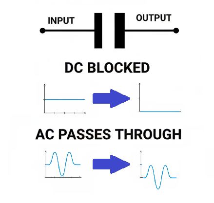
These two properties together make the capacitor the right tool for the first half of the De-Popper problem: isolating DC conditions inside the effect circuit from the signal path during switching transitions.
The capacitor type used for this application varies. I’ve seen film, ceramic, and electrolytics. The typical value is 0.1uF (100nF). I personally would recommend film caps (polyester, polypropylene) for this application.
The Resistor
A resistor opposes the flow of electric current. The relationship between voltage, current, and resistance is described by Ohm’s Law: V = IR. The higher the resistance value, the less current flows for a given voltage.
In this circuit, resistors are used in two distinct roles:
Pull-Down Resistors
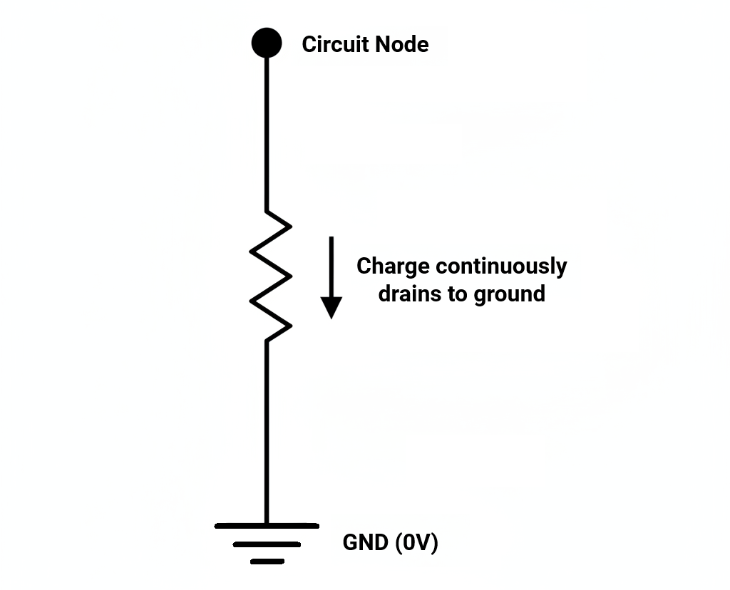
A pull-down resistor connects a signal node to ground. By providing a continuous path for current to flow from the node to ground, it ensures that any charge accumulated at that node drains away continuously rather than building up over time.
In the De-Popper circuit, pull-down resistors are placed at the switch-facing nodes of the coupling capacitors. Any charge that bleeds through the capacitors or accumulates on their plates has a path to drain away to ground through the resistor. By the time the switch transitions, there is no significant DC offset voltage present at the node, and therefore no voltage equalization event … and no pop!
Current-Limiting Resistors
A current-limiting resistor is placed in series between the switch contact and the coupling capacitor. Its purpose is different from the pull-down resistor. Rather than draining charge away, it limits how much current can flow into the capacitor during the switch transition.
By limiting the current, it limits the size of the voltage change that current can create on the other side of the capacitor. The switch bounce still happens and the energy is still injected, but the current-limiting resistor reduces how much of that energy reaches the signal path.
Part 3: Building the De-Popper Circuit
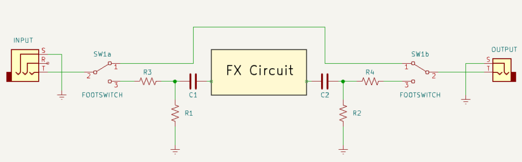
Step 1: Add Coupling Capacitors
Place a 0.1uF (100nF) capacitor in series between the input switch contact and the effect circuit’s input node. This capacitor blocks any DC conditions at the circuit’s input from reaching the switch contact during the bypass transition.
Place a second 0.1uF capacitor in series between the effect circuit’s output node and the output switch contact going to the output jack. This blocks DC conditions at the circuit’s output from the output path during transition.
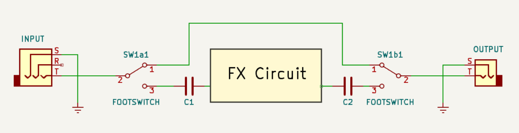
Note: the coupling capacitors alone are not sufficient. While they prevent the circuit’s internal DC offset from reaching the signal path, the capacitors themselves can accumulate charge on their plates while the pedal is in bypass mode. That charge will also equalize at the moment of switching, creating its own pop. The pull-down resistors solve this.
Step 2: Add Pull-Down Resistors
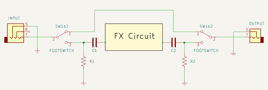
Place a 1MΩ resistor between the input-side switch node (the junction between the switch contact and the capacitor) and ground.
Place a second 1MΩ resistor between the output-side switch node (the junction between the switch contact and the capacitor) and ground.
These pull-down resistors continuously drain any accumulated charge at those nodes to ground. By the time the switch transitions, the charge has bled away and there is no voltage spike to propagate through the signal chain.
The input-side pull-down should be a large value (1MΩ to 2.2MΩ) to avoid loading the signal or reducing the input impedance of the circuit in bypass mode. The output-side resistor is similarly in the MΩ range in most designs, though there are many I’ve seen with 10kΩ – 100kΩ for the output pull-down resistor.
Step 3 (Optional): Add Current-Limiting Resistors
For lower-noise switching – particularly useful of your bypass circuit still exhibits residual pop after adding the capacitors and pull-downs – add current-limiting resistors in series between the switch contacts and the coupling capacitors.
One resistor in series on the input path (between the switch contact and C1), and one on the output path (between the switch contact and C2).
The value of these resistors is design-dependent and typically determined by experimentation. Starting values and the underlying calculation are covered in the supplemental material from Mr. Black Pedals.
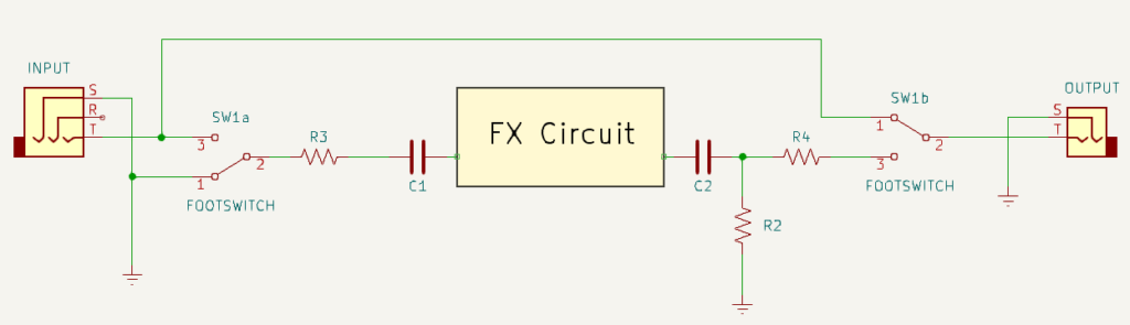
Alternative: The Grounded Input Wiring Scheme
There is an alternative true bypass wiring approach that eliminates the need for the input-side pull-down resistor by connecting the effect circuit’s input to ground when the pedal is in bypass mode. It’s called the Grounded Input Wiring Scheme.
In this scheme, when bypassed, the circuit’s input is tied directly to ground through the switch contact. No floating input, no accumulated charge on the input node – the input side is already at 0V.
This eliminates one component (R1) while achieving the same result. The output-side pull-down resistor is still required. The grounded input scheme is widely used in boutique pedal design.
Parts Lists
The following parts are required for the standard De-Popper implementation (capacitors and pull-down resistors). Current-limiting resistors are optional and design-dependent.
| Ref | Component | Typ. Value | Notes |
|---|---|---|---|
| C1 | Input coupling cap | 0.1uF (100nF) | Film, ceramic, or electrolytic |
| C2 | Output coupling cap | 0.1uF (100nF) | Film, ceramic, or electrolytic |
| R1 | Input pull-down | 1MΩ – 2.2MΩ | 1/4 W |
| R2 | Output pull-down | 1MΩ | 1/4 W |
| R3 | Input current-limiting | Design dependent | Optional |
| R4 | Output current-limiting | Design dependent | Optional |


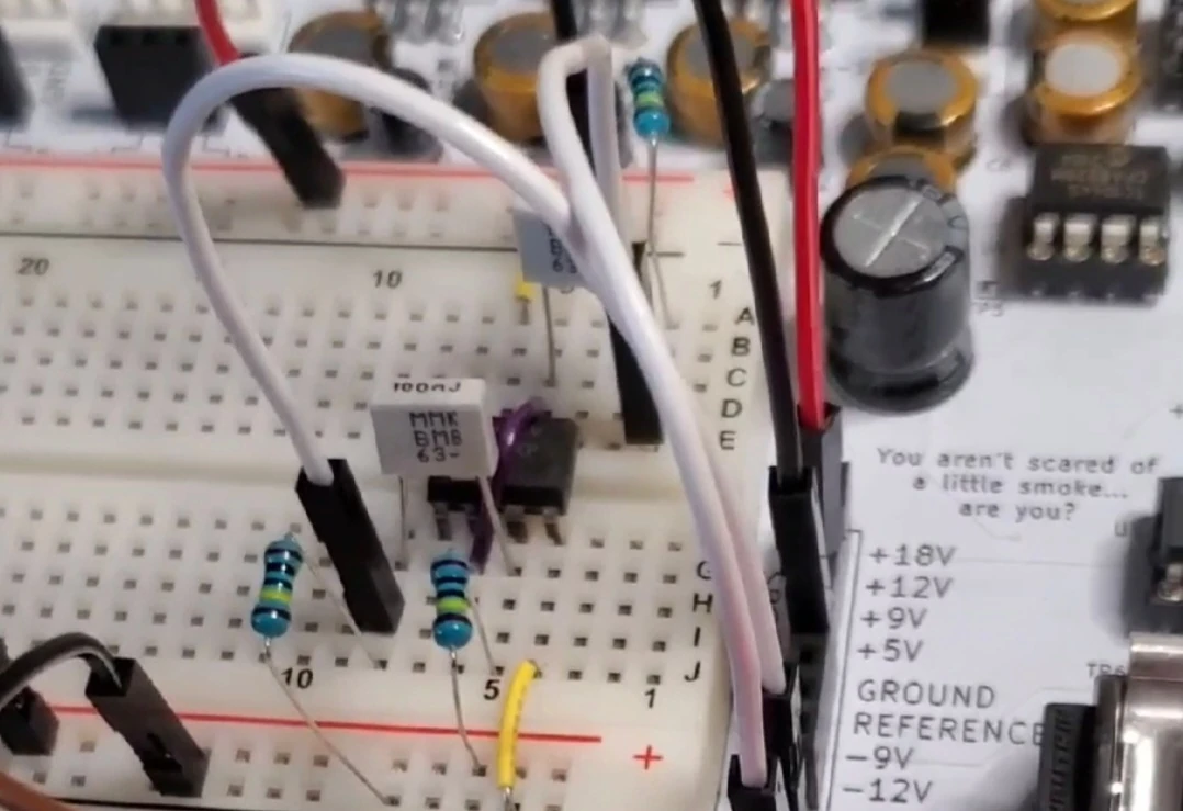
Implementing on the PROTIS 1
The PROTIS 1 development board has true bypass built into its design. To de-pop your breadboarded circuits on the PROTIS 1:
- Place a 1MΩ resistor between the input signal rail and the ground rail on the braedboard.
- Place a 1MΩ resistor between the output signal rail and the ground rail on the breadboard.
- Use a 0.1uF (100nF) capacitor to couple your breadboard circuit’s input to the PROTIS 1 input signal node.
- Use a second 0.1uF (100nF) capacitor to couple your breadboarded circuit’s output to the PROTIS 1 output signal node.
References
[1] Mr. Black Pedals – What really causes switch pop, October 6th, 2012
[2] Jack Orman – Why Guitar Pedals Pop, (C)2015,2017
Guitar Effects Design in 48 Circuits or Less
This post is part of the 48 Circuits or Less series by Stompbox Electronics. Each installment covers one fundamental pedal circuit building block – concept, demonstration, and supplemental resources.
View more articles in this series here.
Meet the Author:

Hi, I’m Dominic. By day, I’m an engineer. By night, I repair and modify guitar effects! Since 2017, I’ve been independently modifying and repairing guitar effects and audio equipment under Mimmotronics Effects in Western New York. After coming out with a series of guitar effects development boards, I decided the next step is to support that community through content on what I’ve learned through the years. Writing about electronics gives me great joy, particularly because I love seeing what others do with the knowledge they gain about guitar effects and audio circuits. Feel free to reach out using the contact form!
The Tools I Use
As a member of Amazon Associates, Stompbox Electronics earns and is supported by qualifying purchases.