

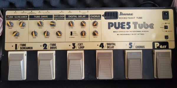
For this edition of Repair Room I take on an Ibanez PUE-5 Tube multi-effects unit. The effect worked, but the switching was completely unresponsive. No change in state, no recalling presets, nothing! Just a brain-dead ON LED staring me in the face. Join me on this Ibanez PUE-5 Tube Repair!

As a member of the Reverb Partner Program, eBay Partner Network, and as an Amazon Associate, StompboxElectronics earns from, and is supported by, qualifying purchases.
Disclaimer: Stompbox Electronics and/or the author of this article is/are not responsible for any mishaps that occur as a result of applying this content.
Ibanez PUE-5 Tube Not Working
Brain-dead. That’s the one word I would use to describe this inoperable Ibanez PUE-5. When the unit is powered up, the “On” LED shines but there’s no reaction to any of the footswitches. I wasn’t even able to bypass the thing!
Troubleshooting the Ibanez PUE-5 Tube
On researching the common problems with the PUE-5 Tube, I found a couple instances of the microcontroller chip being determined as the faulty component. The microcontroller used in this particular unit is a Maxon MC8104H, and it worked in conjunction with a discrete EEPROM chip labeled 80011A.
To test whether the unresponsive behavior was coming from a faulty microcontroller, I needed a schematic. The closest I could find was a service manual that had the schematic for the earlier PUE-5 model (as opposed to the PUE-5 Tube) along with a troubleshooting table. I checked the schematic against the real circuit and it was a surprisingly close fit, so I utilized that as a reference. Better than nothing!
When the unit was turned on, it stayed in bypass mode. Pressing on the bypass switch did nothing. The switch continuity was good, so I looked up which microcontroller pin the bypass switch was connected to (pin 7). Taking a measurement at pin 7, I saw a corresponding change in voltage level. So at least I knew the signal reached the microcontroller pins.
The PUE-5 uses transistor switches to block or pass signals, and the one used for managing the bypass functionality connected to pin 29 (CTRL6). After monitoring that pin and seeing no change in its voltage level, I was convinced that I had encountered a brain-dead multi-effects – i.e. a dead microcontroller.
Ibanez PUE-5 Tube Repair
So from troubleshooting the unit, I knew I needed to find a way to replace the microcontroller chip. The first thing I did was search the web for a spare MC8104H.
This yielded some parts on eBay that didn’t quite look like the chip installed in the unit I was servicing. Instead of replacing it with an existing microcontroller, I decided to use my experience with PIC microcontrollers and design the code from the manual’s functional description.
Not many repairs go this far as to replace the entire microcontroller, code and all. In honest truth this repair took way too much time to perform, but I saw as a cool project moreso than a repair. It also allowed me to brush up on my PIC microcontroller skills.
Hardware Modifications
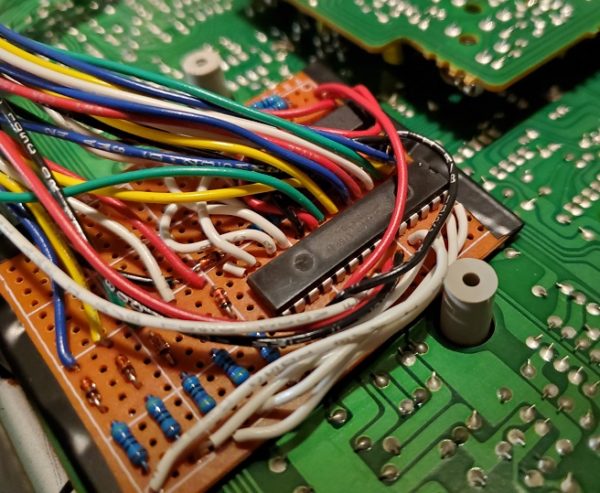
In order to replace the brains I was going to need extensive knowledge on how everything interconnects on the board. I exhaustively routed each pin, determined where it connected and for what it was accountable.
The table below shows what all the pins are responsible for on the stock MC8104H microcontroller. In later sections I break down the basic components and responsibilities in categorical fashion.
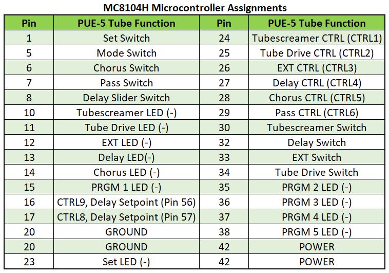
I ended up having to essentially modify the entirety of the microcontroller circuit to have it set up the way I needed it. That meant removing components and cutting traces to isolate electrical interconnects. This process took a while, about a week or so, but I finally got the board to a point where I could comfortably start writing the PIC code.
LEDs and Footswitches
The LEDs are active low, meaning they turn ON when the pin’s voltage is 0V, and OFF when the voltage is 5V. I set up the normally open footswitches as their own independent signals where each switch is pulled up to 5V in the open state with a pull-up resistor.
Delay Time Switch
One interesting component is the slider switch associated with the delay effect. It selects between 1024ms, 256ms, and 64ms delay intervals. A digital processor housed on a daughter board produces the delay effect, and two pins on that DSP chip control the delay interval (pins 57 and 56). The MC8104H microcontroller interfaces with two transistor switches, labeled CTRL8 and CTRL9, which connect to and control those DSP pins.
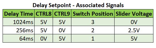
The input from the slider switch is a voltage level, 0V for 1024ms, 2.5V for 256ms, and 5V for 64ms. I took this as an analog input signal and determined the logic using the “Delay Setpoint – Associated Signals” table above.
Transistor Switches
For driving the transistor switches, I used a diode between the microcontroller pin and the transistor gate. The cathode connects to the microcontroller pin and the anode connects to the gate of the CTRLx transistor (“x” being any number from the table above). The transistor switches inhibit signal when 5V is applied to the gate, and allow signal when 0V is applied to the gate.

Microcontroller Hardware
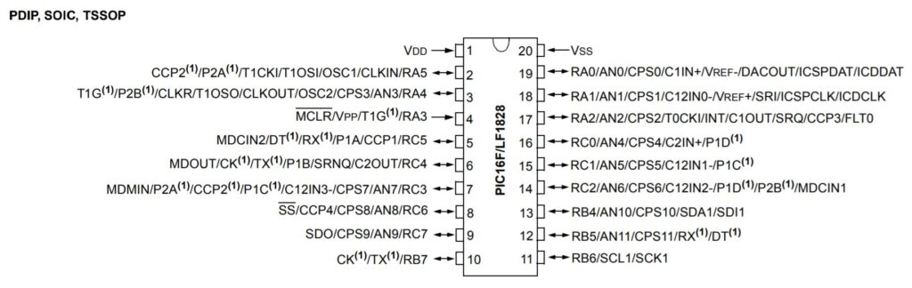
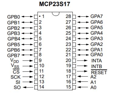
I decided to use a PIC16F1828 for all the input signals and the delay interval controls. I supplemented that with an MCP23S17 I/O Expander to support all the output signals, including the LEDs and transistor switches.
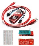
For those who are interested in PIC microcontroller programming, the only device you need to program them is a PICKit. There are a few versions, I personally use the PicKit 3, available on Amazon.
The Code
MPLAB X IDE (with the XC8 Compiler) was used to program PIC microcontrollers, available for free by Microchip.
I will admit, I’m no master of microcontroller programming. I do what I can with what I know, and if it gets the job done in a reasonable fashion, then that works for me. Of course, I’m always looking to improve the way I do things, and one such activity that never stops demanding that is programming. If you come up with a more efficient way to carry out this task, I’m ALL ears!
With that said, the code is located in my GitHub account. The rest of this post will mainly serve as a highlight as to what was done. It also contains some technical info I may want to reference back to in the future.
The General-Purpose I/O (GPIO)
First, we need to define the inputs and outputs. The 16F1828 has the following pinout, from the datasheet:
And the pinout for the MCP23S17:
The tables below show the I/O assignments for the PIC and MCP chips:
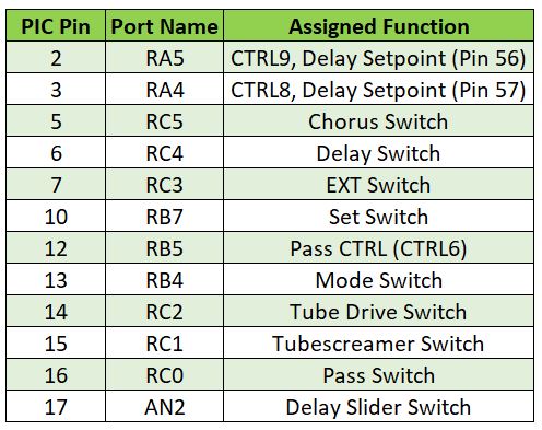
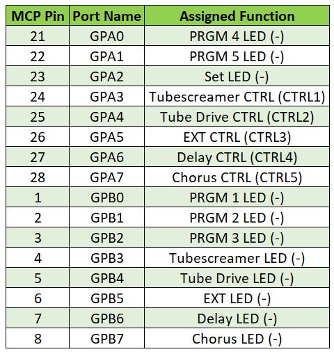
Once this table was built I was able to write up the definitions (‘#define’ statements) for each input and output.
SPI Communications Between MCP23S17 and the PIC
The MCP23S17 I/O Expander communicates with an SPI protocol. That means that if I want an LED to turn on, then I need to send the MCP23S17 a string of bits (in a very specific way) telling it to do so. I’ve worked with the MCP23S17 before (that’s why I picked it) and so I was able to employ some of that code into this project.
The first time working with SPI was not smooth, there are a few picky register settings that need defining in order to operate it.
Initializing the SPI Peripheral
I designated the following:
- RC6 = Chip Select
- RC7 = SDO
- RC8 = SPI Clock
And I configured the SPI peripheral with the code below:
// Initialize PIC SPI Peripheral
SSP1CONbits.SSPEN = 0;
SSP1CONbits.CKP = 0;
SSP1CONbits.SSPM = 0b0000;
SSP1STATbits.CKE = 1;
SSP1STATbits.SMP = 1;
SSP1CONbits.SSPEN = 1;
The first thing the initialization code does is disable the MSSP (Master Synchronous Serial Port) by setting the SSPEN bit to zero. The next two lines respectively set the Clock Polarity to zero and the MSSP to SPI mode with the clock frequency set to a fourth of the internal oscillator frequency.
The SSP1STAT register is set to configure Clock Edge-dependent transmissions and the SPI Data Input Sampling conditions. See DS41419A pg. 290 for the register details. The final step is to reenable the MSSP via the SSPEN bit.
Configuring the MCP23S17
Directly after the initialization code, the MCP23S17 is configured via SPI:
// Configure MCP23S17 SPI I/O Expander Chip
SS = 1; // Turn on chip select
__delay_ms(10);
SPI_Write(IOCON, 0b00101000);
SPI_Write(IODIRA, 0b00000000);
SPI_Write(IODIRB, 0b00000000);
SPI_Write(GPIOA, MCP_GPIOA);
SPI_Write(GPIOB, MCP_GPIOB);
Chip select (SS) is flipped ON, signifying the MCP to pay attention to the microcontroller’s instructions. A little delay is introduced to give the MCP time to adjust itself. Then, five SPI writes are made to the MCP.
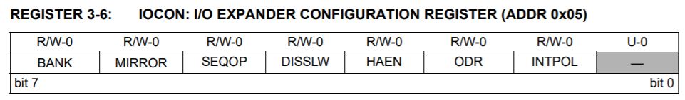
First, IOCON being set to 00101000. When mapped to the register below, we can determine that HAEN and SEQOP are set to 1, while all other bits are cleared. HAEN = 1 enables the MCP23S17’s Hardware Address Pins (A0, A1, and A2) to be externally connected in a user-defined way. I chose to ground all of them to 0V. SEQOP=1 disables sequential operation mode, fixing the address pointer so it does not increment.
The MCP23S17 has two ports: GPIOA and GPIOB, each with 8 pins. The next two write commands set the I/O directionality of each port. In this case, all the pins on both ports are set to Output mode.
The two lines after that reset the GPIOA and GPIOB registers so they hold the register values designated by the variables “MCP_GPIOA” and “MCP_GPIOB”, respectively.
Delay Setpoint Code
For updating the delay setpoint, I wrote the ‘updateDelaySetpoint()’ function and used Analog Input pin 17 (AN2) for sensing the 0V, 2.5V, or 5V provided by the slider switch.
void updateDelaySetpoint(){
  ADCON0bits.GO = 1;
  while(ADCON0bits.GO_nDONE)
    ;
  __delay_ms(20);
  if(ADRESH < 0x1F){
    CTRL8 = 1;
    CTRL9 = 1;
  }
  if(ADRESH >= 0x1F && ADRESH < 0xF0){
    CTRL8 = 1;
    CTRL9 = 0;
  }
  if(ADRESH >= 0xF0){
    CTRL8 = 0;
    CTRL9 = 1;
  }
}
The ADC peripheral starts sampling by setting the GO bit of the ADCON0 register. The while statement is used to wait until the sample is gathered, i.e. until the GO_nDONE is cleared. Once the sample is collected, it is stored in the ADRESH register. Then, short delay of 20ms is introduced for stability.
The delay setpoint is determined by comparing the ADRESH register value to the pre-defined ranges for classifying the position of the delay setpoint switch. Once the voltage range is determined, the delay is set by appropriately configuring the CTRL8 and CTRL9 outputs.
Using the PIC EEPROM Memory for Storing Parameters
The PUE-5 has 5 user-programmable preset configurations available. I used the PIC’s on-board EEPROM for storing and reading presets.
Reading from EEPROM
To read a preset from memory, I created an EEPROM_Read function.
//EEPROM Read Function
unsigned char EEPROM_Read(unsigned char addr){
  EEADRL = addr;
  EECON1bits.EEPGD = 0;
  EECON1bits.CFGS = 0;
  EECON1bits.RD = 1;
  return EEDATL;
}
An EEPROM address is passed into the function which is copied into the EEADRL register. The on-board PIC EEPROM is selected by clearing the EEPGD and CFGS bits. Setting the RD bit initiates an EEPROM read, and the EEDATL is the register whose value now contains the information read from EEPROM memory.
Writing to EEPROM
I defined 5 groups of 2 address locations, spaced 4 bytes apart from each other. Each preset comprised of the MCP_GPIOA and MCP_GPIOB values at the time the preset is saved.
For writing presets, I wrote an EEPROM_Write function:
//EEPROM Write Function
void EEPROM_Write(unsigned char addr, unsigned char data){
  while(EECON1bits.WR){
    continue;
  }
  EEADRL = addr;
  EEDATL = data;
  EECON1bits.EEPGD = 0;
  EECON1bits.CFGS = 0;
  EECON1bits.CARRY = 0;
  if(INTCONbits.GIE){
    STATUSbits.CARRY = 1;
  }
  INTCONbits.GIE = 0;
  EECON1bits.WREN = 1;
  EECON2 = 0x55;
  EECON2 = 0xAA;
  EECON1bits.WR = 1;
  EECON1bits.WREN = 0;

  if(STATUSbits.CARRY){
    INTCONbits.GIE = 1;
  }
  PIR2bits.EEIF = 0;
}
The address and data to be saved are copied into the EEADRL and EEDATL registers, respectively. Clearing EEPGD and CFGS bits configure the EEPROM as the memory source to work with. Clear the GIE (Global Interrupt Enable) to disable all interrupts while performing the write. (If the CARRY bit in the STATUS register is 1, then the GIE should be reset back to 1 – one of the bugs I had to fix…)
Set the WREN bit to enable writing to the EEPROM. Then write to EECON2, first with 0x55, then with 0xAA, as specified in the documentation. The WR bit initiates the write function, followed by clearing the Write Enable bit. Finally, clear the EEIF bit from the PIR2 register to signal an EEPROM-related interrupt is not pending.
Wrap-Up
Overall, this was a fun project with a few hiccups on the way. One of the power regulators failed while testing, and I found one of the switching transistors inoperable as well. Repaired both of those on top of the microcontroller replacement.
Again, you can find all the materials for this project in my Github repo. Thanks for making it this far!
Meet the Author:

Hi, I’m Dominic. By day, I’m an engineer. By night, I repair and modify guitar effects! Since 2017, I’ve been independently modifying and repairing guitar effects and audio equipment under Mimmotronics Effects in Western New York. After coming out with a series of guitar effects development boards, I decided the next step is to support that community through content on what I’ve learned through the years. Writing about electronics gives me great joy, particularly because I love seeing what others do with the knowledge they gain about guitar effects and audio circuits. Feel free to reach out using the contact form!
The Tools I Use
As a member of Amazon Associates, Stompbox Electronics earns and is supported by qualifying purchases.